New research suggests that materials commonly overlooked in computer chip design actually play an important role in information processing, a discovery that could lead to faster and more efficient electronics.
Using advanced imaging techniques, an international team led by Penn State researchers found that the material that a semiconductor chip device is built on, called the substrate, responds to changes in electricity much like the semiconductor on top of it.
The researchers worked with the semiconductor material, vanadium dioxide, which they said shows great potential as an electronic switch. They also studied how vanadium dioxide interacts with the substrate material titanium dioxide and said they were surprised to discover that there seems to be an active layer in the substrate that behaves similarly to the semiconductor material on top of it when the semiconductor switches between an insulator—not letting electricity flow—and a metal—letting electricity flow.
The revelation that substrates can play an active role in semiconductor processes is significant for designing future materials and devices, said study lead Venkatraman Gopalan, professor of materials science and engineering and of physics at Penn State.
"New ideas are needed for smaller and faster electronics in order to keep up with Moore's law," said Gopalan, the corresponding author of the study published in Advanced Materials. "One idea being pursued is materials, such as vanadium dioxide, that can switch between metal—the one state—and insulator—the zero state—states in a trillionth of a second. This is known as undergoing metal-insulator transitions."

The potential of vanadium dioxide as a metal-to-insulator transistor is well-documented and the material is considered promising for semiconductor technology due to its low energy consumption, Gopalan said. However, the material's properties are still not fully understood, and until now, it has usually been observed in isolation rather than while functioning in a real device.
Vanadium dioxide has strongly correlated electronic effects, meaning the repulsion between electrons interferes with the device, so cannot be ignored as is currently done in silicon-based electronics. This characteristic can result in materials with novel functionalities such as high-temperature superconductivity and enhanced magnetic properties.
"The underlying physics of this material is less understood, and its performance in a device geometry is even lesser understood," Gopalan said. "If we can make them work, there will be a renaissance in electronics. In particular, neuromorphic computing—where computer systems that take inspiration from the brains of living systems with neurons—could seriously benefit by using such devices."
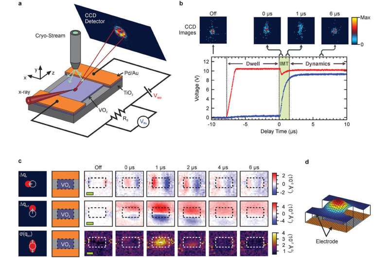
The team investigated vanadium dioxide in a device rather than in isolation, applying a voltage to it to make it switch from an insulating to a conducting state. They used the Advanced Photon Source (APS) at Argonne National Laboratory, which uses powerful X-ray beams to study the behavior and structure of materials on the atomic level. When mapping the spatial and temporal response of the material to the switching event, the researchers observed unexpected changes to the structure of the material and substrate.
"What we found was that as the vanadium dioxide film changes to a metal, the whole film channel bulges, which is very surprising," Gopalan said. "Normally it is supposed to shrink. So clearly something else was going on in the film geometry that was missed before."
The APS X-ray penetrated through the vanadium dioxide film and into the titanium dioxide (TiO2) substrate—which is normally considered an electrically and mechanically passive material—that the thin film was grown on.
"We found to our great surprise that this substrate is very much active, jiving and responding in completely surprising ways as the film switches from an insulator to a metal and back, when the electrical pulses arrive," Gopalan said. "This is like watching the tail wagging the dog, which stumped us for a long while. This surprising and previously overlooked observation completely changes how we need to view this technology."
To understand these findings, the theory and simulation effort—led by Long-Qing Chen, Hamer Professor of Materials Science and Engineering, professor of engineering science and mechanics and of mathematics at Penn State—developed a theoretical framework to explain the entire process of the film and the substrate bulging instead of shrinking. When their model incorporated naturally occurring missing oxygen atoms in this material of two types, charged and uncharged, the experimental results could be satisfactorily explained.
"These neutral oxygen vacancies hold a charge of two electrons, which they can release when the material switches from an insulator to a metal," Gopalan said. "The oxygen vacancy left behind is now charged and swells up, leading to the observed surprising swelling in the device. This can also happen in the substrate. All of these physical processes are beautifully captured in the phase-field theory and modeling performed in this work for the first time by the postdoc Yin Shi in Professor Chen's group."
Gopalan credited the multidisciplinary team's combined expertise in material growth, synthesis, structure analysis and synchrotron beamline operation with the new understanding. Using a collaborative approach led by Greg Stone, a physical scientist with the U.S. Army and the lead experimental author, and Yin Chi, postdoctoral scholar at Penn State and the lead theory author, the researchers disentangled the material's responses and observed them individually using phase field simulations, a simulation that helps scientists understand material changes over time by depicting various states of matter in a virtual setting.
"By bringing these experts together and pooling our understanding of the problem, we were able to go far beyond our individual scope of expertise and discover something new," said Roman Engel-Herbert, director of the Paul Drude Institute of Solid State Electronics in Berlin, Germany, and co-author of the study whose group grew these films along with Darrell Schlom's group at Cornell University.
"Recognizing the potential of functional materials necessitates an appreciation of their broader context, just as complex scientific challenges can only be solved through widening our individual perspectives."
The collaboration enabled both a significant amount of progress to happen in a short period of time and work to be done in a shorter period of time, and brought in a variety of perspectives from multiple disciplines.
The responses themselves require further investigation, researchers said, but they believe that understanding them will assist in identifying previously unknown capabilities of vanadium dioxide, including potential yet-to-be discovered phenomena in the TiO2 substrate that was considered passive before this study. The study itself unfolded over 10 years, Gopalan noted, including validating the results.
"This is what it takes to go from interesting science to a working device you can hold in the palm of your hand," Gopalan said. "Experiments and theory are complex and require large-scale collaborative teams working closely together over an extended period of time to solve difficult problems that could have a large impact. We hope and expect that this will accelerate the progress towards a new generation of electronic devices."
More information: Greg Stone et al, In‐Operando Spatiotemporal Imaging of Coupled Film‐Substrate Elastodynamics During an Insulator‐to‐Metal Transition, Advanced Materials (2024). DOI: 10.1002/adma.202312673
Citation: 'Surprising' hidden activity of semiconductor material spotted by researchers (2024, April 4) retrieved 4 April 2024 from https://techxplore.com/news/2024-04-hidden-semiconductor-material.html
This document is subject to copyright. Apart from any fair dealing for the purpose of private study or research, no part may be reproduced without the written permission. The content is provided for information purposes only.
