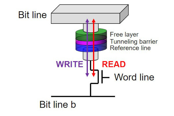
Researchers at Tohoku University have announced the demonstration of a high-speed spin-orbit-torque (SOT) magnetoresistive random access memory cell compatible with 300 mm Si CMOS technology.
The demand for low-power and high-performance integrated circuits (ICs) has been increasing as artificial intelligence (AI) and Internet-of-Things (IoT) devices become more widely adopted. With the present ICs, purely CMOS-based memories such as embedded Flash memory (eFlash) and static random-access memory (SRAM) are responsible for a high proportion of power consumption. In order to lower power consumption while keeping high performance, magnetoresistive random access memories (MRAMs) have been intensively developed. Spin-transfer torque MRAMs (STT-MRAMs) are the most intensively developed MRAM. Major semiconductor companies have now announced that they are ready for mass production of STT-MRAM for eFlash replacement.
Researchers are aiming to replace SRAM with MRAM. For SRAM replacement, MRAM must achieve high-speed operation above 500 MHz. To meet the demand, an alternative MRAM, so-called spin-orbit torque MRAM (SOT-MRAM) was proposed, which has several advantages for high-speed operation. Because of these advantages, SOT-MRAM has also been developed; however, most laboratory studies focus on the fundamentals of SOT devices. To realize SRAM replacement by SOT-MRAM, it is required to demonstrate high-performance of SOT-MRAM memory cell on a 300 mm CMOS substrate. In addition, it is necessary to develop the integration process for SOT-MRAM, e.g., thermal tolerance against 400 °C annealing, which is a requirement of the standard CMOS back-end-of-line process.
The research team led by Professors Tetsuo Endoh and Hideo Ohno—the current president of Tohoku University—has developed an integration process for SOT devices compatible with 55 nm CMOS technology and fabricated SOT devices on 300 mm CMOS substrates. The newly developed SOT device has simultaneously achieved high-speed switching down to 0.35 ns and a sufficiently high thermal stability factor (E/kBT 70) for the high-speed non-volatile memory applications with robustness against annealing at 400 °C. Based on this achievement, the research team has integrated the SOT device with CMOS transistors and finally demonstrated high-speed operation in complete SOT-MRAM memory cells.
These achievements have addressed the issues to make SOT-MRAM practical for commercial applications and thus offer a way to replace SRAM with SOT-MRAM, which will contribute to the realization of high-performance electronics with low-power consumption.
Results will be presented at the 2019 IEEE International Electron Devices Meeting in San Francisco, December 7-11, 2019.
More information: Title: First demonstration of field-free SOT-MRAM with 0.35 ns write speed and 70 thermal stability under 400°C thermal tolerance by canted SOT structure and its advanced patterning/SOT channel technology
Citation: Demonstration of high-speed SOT-MRAM memory cell compatible with 300 mm Si CMOS technology (2019, December 9) retrieved 9 December 2019 from https://techxplore.com/news/2019-12-high-speed-sot-mram-memory-cell-compatible.html
This document is subject to copyright. Apart from any fair dealing for the purpose of private study or research, no part may be reproduced without the written permission. The content is provided for information purposes only.
